|
US Industrial Co.,Ltd
|
circuit board design design circuit board
| Place of Origin: | Zhejiang, China (Mainland) |
|
|
|
| Add to My Favorites | |
| HiSupplier Escrow |
Product Detail
0.6 - 3.2mm&
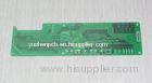
0.6 - 3.2mm Custom Prototype Copper Thickness Circuit PCB Design With Gold Finger
Description:
Printed circuit board artwork generation was initially a fully manual process done on clear mylar sheets. The schematic diagram was first converted into a layout of components pin pads, then traces were routed to provide the required interconnections. Pre-printed non-reproducing mylar grids assisted in layout, and rub-on dry transfers of common arrangements of circuit elements (pads, contact fingers, integrated circuit profiles, and so on) helped standardize the layout. Traces between devices were made with self-adhesive tape. The finished layout "artwork" was then photographically reproduced on the resist layers of the blank coated copper-clad boards.
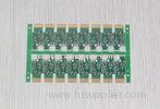
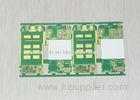
We can help you design any kinds of board as you want, such as: single sided board, double sided board, multi-layer board, FPC, PCBA, aluminum board, led board, mobile board and so on. You just need tell us the use of this board and the size you want. Sample boards will be provided to test before mass production.
Applications:
Printed circuit board can be used for all kinds of electrical products, such as computer, radio, TV, mobile, mp4, led and so on. It’s widely used in various of industries in the world. We have been pcb/pcba business for ten years and provide different customized pcb to many countries all over the world. Welcome to contact us for further news.
Specifications:
|
Product Technical Parameter |
|||
|
Basic technology |
Parameter |
||
|
Single/Double sided |
Multilayer |
||
|
Number of Layers |
1-2 |
4~16 |
|
|
Copper Thickness |
0.25~3.0OZ |
0.5~3.0OZ |
|
|
Base Board Thickness |
0.2~3.2mm |
0.6~3.2mm |
|
|
Incombustibility |
94V-0 |
94V-0 |
|
|
Peelable resistance |
12.3N/cm |
12.3N/cm |
|
|
Twist |
≤0.5% |
≤0.5% |
|
|
Insulation resistance |
≥1011Ω |
≥1011Ω |
|
|
Test voltage |
10-300V |
10-300V |
|
|
Finished board area |
560×970mm |
560×970mm |
|
|
Min. Line Width and Spacing |
0.1/0.1mm |
0.1/0.1mm |
|
|
Copper thickness in hole |
≥25.0um |
≥25.0um |
|
|
Mini. pad diameter |
Inner layer |
US Industrial Co.,Ltd [China (Mainland)]
Business Type:Manufacturer | |